Optical phase-locked loop
Contents
Introduction
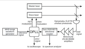
The current version of phase-lock loop is base on this article [1]. The goal is to make a relative optical phase between two lasers to change at a rate  , where
  is beat-frequency and it needs to be in a range from tens of MHz to 7 GHz. As can be seen on a picture
the two lasers are mode-matched and sent to a fast photodetector
, currently we are using Hamamatsu G4176-03. Other variant is New Focus 1577 A photodetector (works up to 12 GHz), although we couldn't achieve the same amount of an electrical signal. After this an achieved beat signal is split between a spectrum analyzer and the phase-lock loop circuit via a directional coupler. The electronic device generates two types of an error signal: fast and slow. Fast part modulates slave laser's current, slow is sent to piezo.
The reference signal is generated with a commonly used signal generator 0-20 MHz. To make this frequency comparable with the beat-frequency, both the beat-frequency and the reference frequency are divided by N and R respectively.
OPLL circuit
OPLL circuit is based on ADF4107 PLL chip [2] and simplified version on a picture.
Phase-lock loop
Capacitors in the loop filter
| Capacitor | Yellow old box for a cavity lock | New box for a cavity lock | Red old box for toptics |
| C4 (piezo and current filter after CP) | 3.3 nF | 3.3 nF | 3.3 nF |
| C13 (piezo integrator) | 470nF | 470 nF | 470 nF |
| C14 (phase advance filter) | 1500 pF | 470 pF | 470 pF |
Old and new PLL comparison
Resistors
| Element | Old (Yellow box) | New | Schematics | Super Old (Toptica) |
| R28 | 50 OMH | 50 OMH | 49.9 OMH | |
| R27 | 10 KOMH | 10 KOMH | 10 KOMH | |
| R26 | 10 KOMH | 10 KOMH | 10 KOMH | |
| R25 | 10 KOMH | 10 KOMH | 10 KOMH | |
| R24 | 230 OMH | 290 OMH | 300 OMH | |
| R23 | 1.39 KOMH | 1.37 KOMH | 1k5 OMH | |
| R18 | 82 KOMH | 82 KOMH | 91 KOMH | |
| R21 | 100 OMH | 100 OMH | 100 OMH | |
| R20 | 200 OMH | 200 OMH | 200 OMH | |
| R19 | 300 OMH | 300 OMH | 300 OMH | |
| R35 | 56 OMH | 56 OMH | ||
| R16 | 8.4 KOMH (?) | 8.4 KOMH (?) | ||
| R13 | 510 OMH | 540 OMH | 510 OMH | |
| R11 | 3.3 KOMH | 3.3 KOMH | 3.3 KOMH | |
| R10 | 3.3 KOMH | 3.3 KOMH | 3.3 KOMH | |
| R9 | 150 OMH | 150 OMH | 150 OMH | |
| R22 | 6.6 KOMH | 6.6 KOMH | ||
| R14 | 7 KOMH (?) | 7 KOMH (?) | 510 OMH | |
| R36 | 510 OMH | |||
| R 12 | 3.3 KOMH | |||
| R 15 | 100 KOMH | |||
| R 30 | 10 OMH | |||
| R 31 | 10 OMH | |||
| R 3 | 150 OMH | |||
| R 4 | 150 OMH | |||
| R 5 | 150 OMH | |||
| R | ||||
| R |
Capacitors
| Capacitor | Old (Toptica) | New (Green) | Schematics |
| C16 | 22uF | 22uF | 20uF |
| C20 | 10uF | 10uF | 10uF |
| C19 | 10uF | 10uF | 10uF |
| C15 | 10uF | 10uF | 10uF |
| C5 | 150nF | 100nF | 150nF |
| C7 | 1uF | 1uF | 1uF |
| C17 | 0.1uF | 22uF | 20uF |
| C21 | 0.33uF | 33uF | 20uF |
| C22 | 0.33uF | 33uF | 20uF |
| C18 | Yellow Shit | 22uF | 20uF |
| C | |||
| C | |||
| C | |||
| C | |||
| C | |||
| C | |||
| C |
Troubleshooting (by Jurgen Appel)
After assembly I recommend to check the following steps to debug the circuit and verify its components:
1) Voltages Check the supply voltages. The circuit should draw <150mA on both +-15V inputs without the LCD connected.
1) LCD Display Upon power-up the backlight should light up.
If it does not, verify that the Voltage on pin 13 of the microcontroller is TTL-High. If it is not, the microcontroller did not start up properly. Is its NotReset-pin (pin1) high? The LCDisplay then shows the Startup-Message. The 10k-Potentiometer R47 is used to set the contrast level of the LCD. On one edge of its range the LCD is just off, on the other side the pixels turn dark. In between you should read text. If instead of the startup-message you see every second text-line filled with dark blocks, the LCD communication failed: Check connections.
2) Quadrature Encoder Upon pressing the encoder pushbutton on the start screen you enter the menu. Once in the menu the pushbutton toggles between select mode (first character of the line is '>') and edit mode (first character is '*'). If pressing the pushbutton does not change between the modes the encoder connections need to be checked. With the encoder not connected the connector pins 1,2,3 should be high (via a microcontroller internal pullup resistor to +5V of ~ 50 kOhms), the encoder is responsible to short the pins to ground. Clockwise rotation should increase edited numbers, counterclockwise rotation decreases numbers. Interchanging the connections to pin 2 and 3 changes rotation direction.
3) Communication to the ADF4107-chip a) To check the communication with the ADF4107-chip the MUX output can be used. In the menu switch the "MUX" setting to 'GND' or 'Vdd' to change the MUX output between 0V and 3.3V.
4) Testing the Reference Input Select the MUX-Output: "R-Divider". After applying a 3 Vpp reference sine wave to the Reference input, on the MUX- output you see the frequency of the reference input divided by the R-setting.
5) Testing the RF-Input
Select the MUX-Output: "N-Divider". After applying a 0dBm input signal to the RF-input, on the MUX-
output you see the frequency of the RF input divided by the N-setting.
6) Testing the Phase comparator Make sure the Charge-Pump is enabled. Depending on wether the RF frequency *N is bigger or smaller than Reference/R the output on X4 (Error) should be either ~0V or ~10V. Changing the charge pump CPPolarity (CPPolarity) negates the output.
7) Testing the FET output The FET-Output follows the ERROR-Signal. It's amplitude can be changed by the 10-turn potentiometer.
8) Testing the Integrator output When changing the Charge-Pump polarity the integrator output should run high or low in ~ 1/5 s after opening the toggle switch. The LED lights red or green.
9) Putting things together: Locking for the first time: Disable the FET-Lock by setting the 10-turn potentiometer to minimum gain. When scanning the Laser over the lockpoint over ~ 100MHz with ~ 10Hz the Error-Signal should switch from 0 to 10V in an almost rectangular fashion. If the FET gain now is slowly increased a horizontal step at 5V should appear. If not, try inverting the CPPolarity setting.
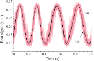
10) Now disable the FET-Lock by setting the 10-turn potentiometer to minimum gain again. Lock the laser using the piezo output: The laser should oscillate around the lockpoint. If it is driven away from the lock point, invert the piezo polarity. Now increase the FET gain: The laser should lock. The Error-signal should change from a 10Vpp trapezoid signal to a noise signal of a few mV only.
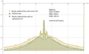
Use a spectrum analyzer to monitor the spectrum of the beat signal. Try minimizing the sideband noise power by a) trying a different balance between CPGAin and the 10-turn-potentiometer setting. b) trying different values in the range 47 pF .. 220 pF for C14. C13 and C4 normally do not have to be changed.
If the error signal mostly is in the mV range but shows narrow "spikes" on an analog scope in 500µs/div time scale this signifies phase slips. Most often the cause is insufficient RF power in the beat signal. Optimize by improving mode matching, increasing optical power or adding amplifiers.
Our experimental parameters and typical problems
- Power of each laser is ~3mW. Polarizations should be the same.
- The beat signal power should be around 0 dBm, if it is getting too low the laser will be locked at a wrong frequency
- If there is no error signal, usually ADF4107 is damaged. Check pin # 2
- It is possible to burn a micro-controller, then reprogram using the following section
Reprogramming ATMEGA168
How to program (or reprogram) a microcontroller for Laser PLL Box (the section is written by Paul Herringer, August 2016)
You need the pocket AVR programmer from Sparkfun. Make sure that the drivers are installed, and that you know how to use the programmer - instructions can be found by googling "sparkfun avr programmer" and navigating to the hookup guide.
Check that AVRDude is installed. Connect the programmer and in a command line window type "avrdude -c usbtiny". If AVRDude is installed it should tell you that you need to specify an AVR and give a list of codes for supported AVRs. The AVR used in the PLL Box is an ATMega 168, for which the code is m168. If AVRDude isn't installed, either install Arduino (which should include AVRDude) or follow the link on this Sparkfun page about AVRDude: https://learn.sparkfun.com/tutorials/pocket-avr-programmer-hookup-guide/using-avrdude
Put the microcontroller to be programmed in an Arduino Uno Board, and connect it to the computer using the pocket programmer. In command line, cd to the folder where 'laser_pll_flash.bin', 'laser_pll_eeprom.bin', etc are saved (should be the same folder as these instructions). There should be a one file each for flash, eeprom, hfuse, lfuse and efuse. Then type "avrdude -c usbtiny -p m168 -U memory_type:w:filename.bin" to write each type of memory to the microcontroller.
For example: "avrdude -c usbtiny -p m168 -U flash:w:laser_pll_flash.bin" to write flash memory.
Last time I did this, AVRDude wouldn't write efuse and lfuse, presumably because the files are empty since the new microcontroller worked fine. However I kept all the files in the folder just in case I'm wrong about that.
The microcontroller should now be programmed. Disconnect from the Arduino board and put it back in the lock box.
If for some reason the program files are lost, you can read them off a working microcontroller (which is how I got them in the first place).
The general command for reading memory in AVRDude looks like this: "avrdude -c usbtiny -p m168 -U memory_type:r:filename:r". If the file doesn't exist already it should get saved to your user folder.
For example "avrdude -c usbtiny -p m168 -U flash:r:backup_flash.bin:r"
Do this for each memory type to get all the files needed for a new microcontroller.
I figured out how to do this from the page at https://www.hackster.io/rayburne/avr-firmware-duplicator-115d8f. There is a program available there that would automate this process but for duplicating a small number of microcontrollers it didn't seem worth the trouble of getting it installed. There is a good explanation of how everything works though if I have left anything out.
Lock performance
Here I at first post the results observed by Jurgen Appel, when they published the article. For our measurements we used Rohde&Schwarz SMB 100A signal generator. From the datasheet SSB phase noise for the carrier frequency f=100 MHz, the carrier offset 20kHz noise is -141 - -145 dBc.

Necessary components
| Component | partial number | where to order? |
|---|---|---|
| directional coupler | tyco 2020-6617 | ebay, used |
| photodetector | Hamamatsu G4176 |


